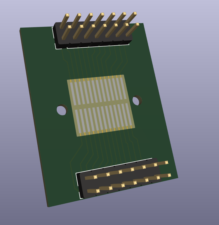
Designing Reliable Compression Contact Interfaces
When using elastomeric connectors, the PCB footprint is just as important as the connector itself. Unlike soldered connectors, elastomeric connectors rely on controlled mechanical compression between conductive elements and the PCB contact pads. Proper footprint design helps ensure consistent contact resistance, reliable alignment, and long service life.
This application note outlines recommended PCB layout practices for linear elastomeric connectors. While the dimensions shown use a 1.00 mm pitch as an example, the same design principles apply to virtually any connector pitch or contact count.
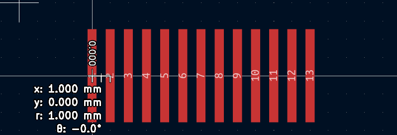
Example PCB Footprint (1.00 mm Pitch)
The example footprint illustrates a typical land pattern for a 1.00 mm pitch elastomeric connector. Important dimensions include:
- Contact pitch
- Pad width
- Pad length
- Solder mask opening
- Connector outline
- Alignment features
These dimensions should always be reviewed against the specific connector drawing for your application.
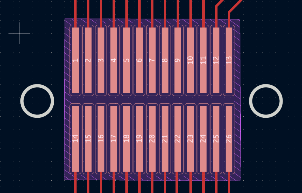
Recommended PCB Land Pattern (Example: 1.00 mm Pitch)
The dimensions below represent the recommended PCB land pattern for the 1.00 mm pitch example presented in this application note. Pad dimensions and spacing may vary depending on the connector pitch, contact geometry, compression requirements, and overall application.
| Parameter | Example Dimension | Notes |
|---|---|---|
| Pad Width | 0.70 mm | Provides generous contact area while maintaining adequate spacing between adjacent pads. |
| Pad Length | 4.00 mm | Recommended for reliable contact and alignment tolerance. |
| Pad Pitch | 1.00 mm | Center-to-center spacing between adjacent pads. |
| Solder Mask | None over contact pads | Contact pads should remain fully exposed. |
| Solder Mask Between Pads | None | Eliminates raised solder mask that can interfere with compression. |
| Surface Finish | ENIG, ENEPIG, or Hard Gold | Recommended for low contact resistance and long-term durability. |
Design Notes
The land pattern shown above is intended as a reference example for a typical 1.00 mm pitch linear elastomeric connector. Other connector pitches—including 0.50 mm, 0.80 mm, 1.27 mm, and custom geometries—may require different pad widths, lengths, and spacing. Always refer to the connector drawing or consult Z-Axis Connector Company when designing a footprint for a specific application.
Contact Pad Geometry
The PCB pads provide the electrical interface between the connector and the circuit board.
For best performance:
- Use rectangular contact pads.
- Maintain consistent pad dimensions throughout the connector.
- Avoid sharp corners or irregular pad shapes.
- Ensure adequate contact area without unnecessarily increasing pad size.
A properly sized pad provides reliable electrical contact while accommodating normal manufacturing tolerances.
Maintain Consistent Pitch
The center-to-center spacing of each pad should match the connector pitch precisely.
Maintaining uniform spacing ensures that each conductive element aligns correctly with its corresponding PCB pad.
Whether using 0.50 mm, 0.80 mm, 1.00 mm, or larger pitches, consistent spacing across the entire footprint is essential.
Solder Mask Clearance
The connector should compress directly against the PCB contact pads—not against raised solder mask.
Recommended practices include:
- Pull the solder mask back from each contact pad.
- Use uniform solder mask expansion.
- Avoid raised solder mask edges within the contact region.
Proper solder mask clearance improves contact consistency and reduces the risk of intermittent electrical connections.
Surface Finish
Since the connector repeatedly contacts the PCB surface, a durable finish is recommended.
Typical finishes include:
- ENIG
- ENEPIG
- Hard Gold
These finishes provide excellent corrosion resistance, low contact resistance, and long-term durability.
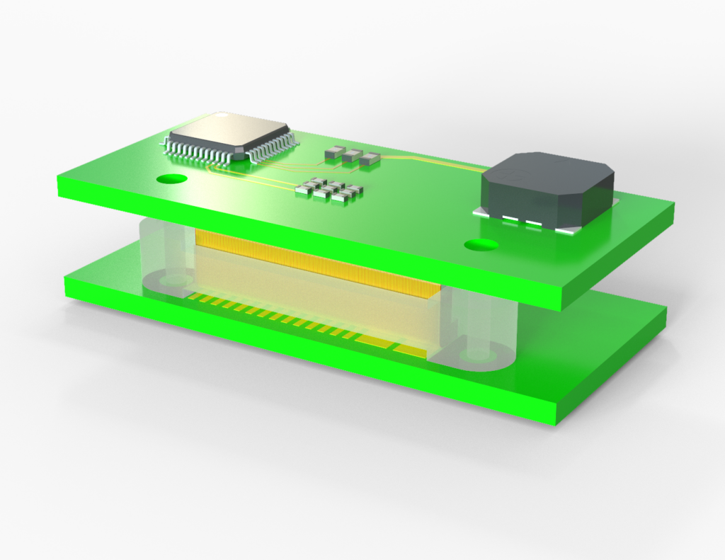
Mechanical Alignment
Electrical performance depends heavily on proper mechanical alignment.
Depending on the application, consider incorporating:
- Alignment pins
- Machined locating pockets
- Mounting holes
- Connector guide features
Good alignment reduces assembly variation and improves repeatability during installation.
Compression Control
Elastomeric connectors are designed to operate within a specified compression range.
Too little compression may result in increased contact resistance or intermittent connections, while excessive compression can reduce connector life.
A rigid housing or fixture should include a positive mechanical stop to ensure repeatable compression during assembly.
Design Checklist
Before releasing your PCB layout, verify the following:
- Correct connector pitch
- Proper pad geometry
- Adequate solder mask clearance
- Recommended PCB finish
- Alignment features incorporated
- Controlled compression using a mechanical hard stop
- Connector outline verified against mechanical drawings
Final Thoughts
A well-designed PCB footprint is essential for maximizing the performance and reliability of an elastomeric connector. By carefully considering pad geometry, solder mask clearance, mechanical alignment, and compression, designers can achieve repeatable, low-resistance electrical connections across a wide range of applications.
If you are designing a new product and would like a footprint review, the engineering team at Z-Axis Connector Company can provide recommendations tailored to your specific connector geometry and application requirements.